Hi DJ,

I am not sure if it helps. I have posted something
similar earlier,
http://archives.seul.org/geda/user/Jan-2009/msg00056.html
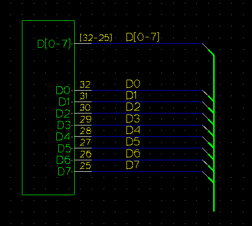
May be some pages in that example have similarity to
your screen shot example?

That example was based on none-flat hierarchy, however,
its not difficult to have the gnet-xxx.scm to flatten
it for flat-netlist.  From my experience, most advance
EDA tools can use the same schematics to produce
none-flat hierarchy netlist for VLSI or flat ones for PCB type
of application. In gEDA case, all the informations are
there to produce flat or none-flat by gnetlist C/SCM.
Its the matter of attribute processing by the
gnet-xxx.scm similar to gnet-verilog.scm.

If I understand it correctly, you would like to see
the top portion of your screen shot's symbol, but
have them netlisted as if its the bottom? If thats the
case, it should not be difficult.  But if you want
both to be shown on schematics and netlist only
the bottom, I have to think about it.

Best Regards,
Paul Tan


-----Original Message-----
From: DJ Delorie <[email protected]>
To: [email protected]
Sent: Thu, 8 Jan 2009 10:22 pm
Subject: Re: gEDA-dev: Google Summer of Code 2009


> I know you are very busy and its very difficult to discuss all the
> details. Do you think an example, or a screen shot may help?

In my case, what I want is pretty simple to show.  I want these to be
equivalent: http://www.delorie.com/pcb/djbus.png

The netlister backends should always see the "demultiplexed"
connections.  I.e. they'll see the top net/pin connection as if you'd
done the bottom set of connections.

I don't care about the syntax or mechanism, as long as I don't have to
draw N pins/nets to denote N electrical connections for an N-bit bus.


_______________________________________________
geda-dev mailing list
[email protected]
http://www.seul.org/cgi-bin/mailman/listinfo/geda-dev


_______________________________________________
geda-dev mailing list
[email protected]
http://www.seul.org/cgi-bin/mailman/listinfo/geda-dev